The new
generation of Solid State Tesla Coils
Project Goals:
>1m Sparks, 400kHz
|
QCW Tesla Coil
 The QCW, or Quasi-Continuous-Wave DRSSTC is a variant of the Double
Resonant Solid State Tesla Coil and is characterized by its ability to
make long, straight sparks usually more than 10x the length of its
secondary. The QCW was first conceived and implemented by Steve
Ward in around 2009/10 or so, around half a decade after the invention
of the DRSSTC (generally accredited to the work of Steve Ward, Steve
Conner & Terry Fritz). To date (2013), it remains the newest and perhaps
most interesting Solid State Tesla Coil variant. With the success of my
previous electronic coils (also see my SSTC 1,
SSTC 2, DRSSTC 1 and
DRSSTC 2), building a QCW is the logical next
step. The QCW, or Quasi-Continuous-Wave DRSSTC is a variant of the Double
Resonant Solid State Tesla Coil and is characterized by its ability to
make long, straight sparks usually more than 10x the length of its
secondary. The QCW was first conceived and implemented by Steve
Ward in around 2009/10 or so, around half a decade after the invention
of the DRSSTC (generally accredited to the work of Steve Ward, Steve
Conner & Terry Fritz). To date (2013), it remains the newest and perhaps
most interesting Solid State Tesla Coil variant. With the success of my
previous electronic coils (also see my SSTC 1,
SSTC 2, DRSSTC 1 and
DRSSTC 2), building a QCW is the logical next
step.
However, the design and construction of a QCW is generally regarded to
be more challenging and difficult than any other SSTC variant, and there
is not much information online on its principle of operation,
construction details etc. Thus my goal for this project is
two-fold. [1] To create a comprehensive document on the operation,
design and construction of a small and relatively simple QCW coil, and [2] to serve as a learning
project. I expect to face difficulties throughout the
project, but I know it will be a good learning experience.
At time of writing (mid-Oct 2013), the QCW DRSSTC is still indeed
somewhat of a rarity. As far as I know from forums and such, Steve Ward
remains the leader in this field with his excellent bus-modulated QWC (the original, which plays to his electric guitar), as well as Zrg's impressive 'Junky QCW' (which holds the record for
longest spark length of 230cm with a 25cm tall secondary). I've created
a small list of what I would call the pioneering few QCWs in the world
at the bottom of the page. After browsing various forums, there seems to
be around 10 or so of such coils in existence. This should make my QCW 1
to be one of the first in the
South East Asian region, or even in Asia!
Finally, I note that there are several variants of QCW coils, including
the newer 'phase shifted' bridge topology. This project focuses more on
the original bus modulated QCW, but I will also explain some of the
newer methods of QCW operation below.
Update (Sept 2014) - QCW 1 has been finally put
together and has achieved its original goals of 1m (40") of spark with a
5.5" secondary, which is greater than 7x secondary length, all with just
a 150V ramp. My components have the ability to go up to 300V or more, so
the new stretch goals for the project will be 10x secondary length of 55
inches (140cm), and then to fit it all together in a nice enclosure.
Thanks for
visiting my page! If you have any questions, wish to share your
projects, or feel that my projects have inspired you in one way or
another, feel free to email me at loneoceans[at]gmail(dot)com. I'd love
to hear about your projects too!
Page Contents
1. QCW Introduction
2. Constructing the QCW (DRSSTC)
3. Constructing the QCW (Buck Bus Modulator)
4. Results
5. Credits and Links
Specifications for QCW 1 (updated Sept 2014)
-
IRGP50B60PD1 Dual Full Bridge Inverter 'easyBridge v1.0'
- 12.8nF Mica 6kV 40Arms Resonant Capacitor
- 60N60C2D1 Dual IGBT + ISL9R3060 diode asynchronous Buck Converter
> Might upgrade to dual 50B60 IGBTs with a
FFH75H60S diode
- ATtiny45/85 for ramp generation and interrupter control
- 100A primary current (150A max)
- 100cm spark goal (140cm stretch goal)
- UD 2.7A, My own modification of the UD2 driver
- 9 x 14cm secondary (or 3" x 5.5")
- 60-degree conical primary
- 8 x 2" Spun Toroid
- About 400khz secondary frequency unloaded
- Max 340VDC on the bridge (240V rectified)
- 10 - 20ms ramp time
- Large bus capacitance (>= 6800uF)
Schematics
Here are the schematics for my QCW 1. Note that these
are still experimental and subject to more changes!


Universal Driver 2.7 for DRSSTC Driver and my QCW
Buck Controller V1.0

Schematic for my new 8-IGBT bridge layout
For much more videos and images of the coil in action, please scroll down to
Results!
25 Oct 2013
1. Introduction and Goals
The newest frontier of Tesla Coils in the modern age is
the QCW DRSSTC, capable of generating huge, long sparks with some clever
drive techniques. Having built several successful coils, I wanted to try
my hand at a more advanced project. In this writeup, I assume the reader
has a good understanding in basic DRSSTC operation. For more
information, do check out my other DRSSTC pages.
What is a QCW and how does it work?
A QCW (Quasi Continuous-Wave) Tesla Coil is a variant of
the Double Resonant Solid State Tesla Coil (DRSSTC), characterized by
long-pulse durations and a high impedance primary circuit. The input of
the inverter is fed via a
gradual ramp of the bus voltage. This results in what
appears to be a very efficient spark propagation, leading to very long
sword-like sparks with incredible spark lengths compared to the secondary coil.

Pioneering QCW work by Steven Ward, Jan 2010, which has been refined
and improved over the years.
The first QCW was first built by Steve Ward in
2008/09. The principle of operation was based on the observation that
long straight sparks could be obtained in Vacuum-tube Tesla Coils when
they were running in staccato mode.

In this mode, the VTTC is
powered on in sync with the rising quarter input AC wave-form
from the mains. The above diagram shows how the interrupter (blue)
signal might look like, with the bus of the inverter powered by the
rising slope of the mains AC wave. I demonstrated this principle in my
Ramped SSTC, producing similar spark
characteristics. This led to the hypothesis that gradually increasing the
bus voltage throughout the duration of the spark would be conducive for huge spark growth.
In a VTTC or a ramped SSTC, we are limited by the period of the AC wave,
thus placing a limit on the maximum ramp duration and how big we can
'grow' our spark. The
second observation was that coils running at 300kHz or higher generate
sparks that tended to
become straighter and straighter. Combining these two ideas together produced
the QCW.
In a classic DRSSTC, the primary is energized for only
several RF cycles (around 10 or so). Due to the resonance and
low-impedance of the primary circuit, primary current rings up quickly
to several hundreds of Amps in a matter of several hundred micro-seconds
(e.g. 70-150us in my DRSSTC 2). In a QCW, the rise time occurs over
several milli-seconds instead (e.g. 10 to 20ms), which is some two
orders of magnitudes greater. In order to prevent the current from
ringing up too high, a high impedance primary circuit is required. This
translates to a primary coil with large inductance (this results in high
coupling) and a small resonant
capacitor. The primary current is usually kept around 100 to 200A
(limited by the bus modulator). The
highest at time of writing is Zrg's coil
running at 300A with a dual full-bridge making 2.3m sparks.
According to simulations and some measurements carried
out by Steve Ward, the actual voltage produced at the top of the
secondary coil doesn't exceed more than several 10s of kV (around 50 -
70kV). It appears that the streamer grows well as energy is pumped in
over the course of each pulse duration, and the spark growth is guided
by the electric field around the toroid.
Thus to summarize, the QCW is characterized by:
- Resonant frequency of at least 300kHz (higher than
400kHz and it becomes more and more difficult to switch the IGBTs)
- High impedance primary (coupling of >=0.3, many turns for
primary and with a small tank cap of around 8 - 15nF)
- A gradual linear bus voltage switched by the inverter over a 10 to
20ms duration
- Relatively large toroid to stabilize the frequency deviation caused by
a large streamer (acts to increase capacitance of secondary and lowers
fres)
There are currently three main methods to achieve the
QCW effect. The first method is via some sort of
bus modulator, which needs to be capable of feeding a
linear
voltage input to the bridge inverter at 100 - 200 Amps. This is
implemented as a high power buck converter. The big challenge is that
the buck converter
needs to be able to supply the current required by the bridge,
and the physically large filter components (inductor and capacitor)
required. However, if a suitably powerful buck converter can be made,
then we can potentially produce the best results since the inverter transistors are soft-switched. Therefore this
method is also best suited to scaling up.
The second method is via a
phase-shifted bridge. In this topology, the inverter bridge driving the
primary coil is not working in perfect opposition, but rather in a
modulated shift over time. This achieves the same gradual voltage rise across the
primary circuit, and consequently does away with the need for the
physically large buck
converter. However, half of the transistors of the bridge are being hard-switched (versus
zero-current switching in the previous method), which requires a very
robust bridge design with proper thermal management due to much higher
switching losses. Consequently, the transistors are being driven to their
edge. Steve and Phillip have both tried this approach and strung several bridges (and primaries) in parallel
to handle the hard-switched current. This uses many expensive transistors but is known to produce good
results in a compact size. In the phase-shift topology, there is a limit to the current handling capability of the
hard-switched transistors, making scaling up challenging (it seems like
a 16-transistor bridge is the largest at the moment). One way this can
be improved is to alternate the hard switching among the transistor
pairs. This method requires some clever circuitry and arguably more
complex to implement.
The third method is
Delta Sigma modulation proposed by Steve Conner, whereby a
conventional DRSSTC controller with a over-current detector is used.
This over-current detector's reference comparator is fed a ramp input,
so the result is more like a 'PWM' control and the current ramps up
proportionally to the over-current ramp signal. However, there hasn't
been any proper working models demonstrating this concept at the time of
writing. Note that this method ramps the current up linearly (with a
linear ramp), as opposed to a linear voltage ramp for the other
two methods.
In order to keep the costs of the project down and to
make the circuit as simple and elegant as possible, I have opted for the
buck-converter topology. The difficult part now lies in building a
suitable buck converter, since the rest is no different from a normal
DRSSTC (other than some parameters).
QCW 1 Project Goals
Because this will be my first QCW Tesla Coil, I plan to
keep the design as simple and straightforward as possible, whilst not
being overly ambitious in terms of is performance for the purpose of
reliable operation.
Project Goals
- Produce sparks of at least 1 meter (39")
- Using a secondary coil of around 6"
- Show reliable operation
- Planned running frequency of 0.5Hz to 5Hz
- Operate at 300V max
- Be reasonably compact
With the goals set, it is time to get started!
2. Constructing the QCW - High Z DRSSTC
October 2013
The QCW (buck driven design) can be broken down into two large
components: the DRSSTC, and the Bus Modulator. The first part is
constructing the DRSSTC. A QCW calls for a high impedance (Z)
coil. Building these two components separately allows me to test
the system in two major modules.
Secondary Coil
The goal of a QCW coil is to produce very large sparks from a
small Tesla Coil, so this motivated me to design a secondary
which was reasonably small, yet maintain a resonant frequency
around 300 - 400kHz which is optimum for spark growth. I had
some spare 3" PVC (which has a 3.5" Outer Diameter) pipe around,
so I decided to use that for my coil form. I also decided to use
a 8 x 2" aluminium toroid for the coil. Using JAVA TC, I found
that winding the coil with AWG 32 for a length of around 5.5
inches would give me a resonant frequency of around 320kHz with
the topload. Therefore, the secondary coil was wound by hand
using a simple makeshift coil winder I built with some scraps of
wood.


I also cut out some around acrylic pieces (6mm thick) which I
then threaded with 2-56 holes which screw onto the coil as end
caps! These were later threaded in the middle to accept a 1/4-20
bolt where I could screw the secondary to the base and the toroid.


The winding proceeded smoothly and was done in little over half
an hour. I gave the coil 3 coat of clear polyurethane. Now it
turned out that the insulation of the wire was thicker than I
expected and therefore quite significant, and the resonant frequency of the
secondary coil with toroid turned out to be closer to 400kHz!
This was somewhat out of spec and I might need to make a new
coil form if it does not perform well. However, with a simulated
3 foot long wire as a streamer, the streamer capacitance brought
the resonant frequency of the secondary closer to 320kHz. One
good thing about the higher frequency is that more power can be
put into the spark, and that higher frequency usually leads to
straighter sparks. I might make another lower frequency coil to
see how that performs.
Primary Coil
For the Primary Coil, I designed and laser cut supports which
will accept some normal stranded 14 AWG wire I had around. The
wire is slightly thin, but given the relatively low (in DRSSTC
land) peak currents of 100A that I plan to run the coil at,
along with the low duty cycle, it should be sufficient for now.


It's great to have access to a laser cutter! The primary coil
was designed with the following specifications:
-
5.1" Innermost diameter
- 60 degree inverse conical shape
-
Capability of up to 12 turns for the primary
- Press-fit accepting 14 AWG stranded wire from HomeDepot
-
Around 7.4" diameter at height of 1.85" for the 10th turn
-
k of around 0.33 for 9 turns
The result of this gives me a coupling coefficient of around
0.32 to 0.35k depending on the number of turns I decide to
use eventually, which is great for a QCW.


Coupled with my 12.8nF tank capacitor, the resonant frequency
can be adjusted all the way down to around 270kHz at turn ~12,
and anything higher to match! For example, turn 8.5 gives me a
primary resonant frequency of around 360kHz and 8 around 390kHz.
The primary coil turned out very well (acrylic piece were glued
with a solvent acrylic glue, probably some sort of
chloromethane).

The completed primary coil with 60 degree inverse cone
geometry and 14AWG wire.
As mentioned, the first secondary coil I made turned out to have
a higher than expected resonant frequency. This can be fixed by
winding a new coil, adding some capacitance (e.g. larger toroid),
or alternatively, just tuning the primary to a higher resonant
frequency.

For tapping the primary, I found it best to simply cut segments
of the insulation on the wire off. I also made a brass tap which
allows me the clamp the primary return wire on. Finally, another
thing to note about QCWs is the characteristically low
top-voltage. According to measurements done by Steve Ward, it
seems that the voltages on a QCW are only on the order of
several tens of kV (50 - 70kV), and the amazing spark length is
caused by 'growing' the spark. This allows us to use very high
coupling without any flashover. The high coupling also causes
the poles of the resonant system to move apart more - more on
this later.
The Resonant Capacitor
The resonant tank capacitor of a DRSSTC is usually made from several
small polypropylene film capacitors (hence the name Multi-Mini Capacitor
or MMC), usually of the CDE 940/942 variant. For QCW, the tank capacitor
needs to sustain long pulses and several thousand RF cycles, and
therefore need to be low-loss and have an excellent RMS rating.
In addition, the high impedance primary (to keep the primary
currents reasonably low throughout the long pulse duration)
allows the use of a lower voltage capacitor. However, it must
have high RMS current handling capability since
we will be running several thousands or more of RF cycles per
pulse.


Thus for a QCW, we need a tank capacitor of the following
features:
-
High RMS current handling
-
Generally low capacitance to increase primary impedance
A capacitor of 8 to 15nF is typical in QCW coiling use to keep
the primary impedance low. Polypropylene film capacitors will
probably be ok for QCW use but they can get hot due to the high RMS
currents at high duty cycles. The best capacitor of choice is therefore
the Mica capacitor.
However, they are difficult to find and expensive! Fortunately, I managed to pick up a few
of them at a local swap-meet for $5 each! These are very nice
20A RMS capacitors, being 10nF and 18nF at 4kV and 2kV
respectively. Together, they form a 40RMS 12.857nF 6kV capacitor
bank, measured at 12.87nF.

12.87nF Mica resonant capacitor rated 40A RMS at 6kV,
with full bridge inverter (this was later replaced with a bigger
bridge).
The capacitor measured out at 12.87nF as expected (Mica caps are
usually made with very high accuracy). Brass bars were machined
to hold them together and act as terminals.
Measuring the Resonant Frequencies
I decided to do a quick test to measure the actual resonant
frequencies of my system.


First up was testing the resonant frequency of the secondary
coil with the slightly-smaller-than 2x8" toroid in place. As
mentioned it turned out that the resonant frequency of the
unloaded secondary seems to hover around 406 - 409kHz, which was
higher than I had expected. However, added a simulated streamer
(wire) at the top about 2.5 feet long dropped the resonant
frequency to 321-326kHz.


Next I hooked up the MMC to the primary and proceeded to test
the resonant frequency of the primary with the secondary coil in
place. At turn 9.5, the primary showed a resonant frequency of
323kHz. This increased to 355kHz at turn 8.5.

Finally, I sent a square wave signal to the primary and measured
the resonance of the whole system by hanging the scope probe in
the air attached to a piece of wire to find the resonant
frequency of the system at turn 8.5 on the primary. This gave me
384kHz. The values here are documented for reference.
New Toroid (2014)
I managed to get a new toroid which measures 2.1" x 8", larger
than the previous 1.9" x 8" toroid, which looks nicer,
and helps also in terms of lowering the secondary
resonant frequency.

This gave me a secondary resonant
frequency (with pri coil in place) of about 392kHz. Two
of the same toroids stacked on top of each other gave 361KHz,
and adding a half meter long wire to simulate streamers dropped
the frequency down to 339kHz. The primary should resonate at
around 390kHz at turn 7.5. With a k = 0.32, this should give a
lower pole at 340kHz.
As far as tuning goes for a QCW, I'm not exactly sure what the
best way is so I'll keep this section as a reference for
now.
The Full Bridge Inverter (Old Version)
*Update 2014 - the single transistor full bridge has
been updated to a better dual-bridge. See below for the new
inverter*
The QCW is simply a variant of the DRSSTC. Since we're looking
to maximize power for a QCW, a full bridge makes the most sense
(although there is no reason why it wouldn't work with a half
bridge). For my full bridge (I'll be interchangeably using the
term inverter), I decided to go with the tried and tested
ultra-fast FGA60N65SMD IGBTs in a TO-247 package. They are
especially
fast IGBTs even at 300kHz+, which are important since unlike
normal DRSSTCs which run from 5 to 10 RF cycles, QCWs run for
thousands of cycles, and heating losses (per burst) become a big
issue. I have also used these IGBTs in my
DRSSTC 1 with fantastic results and very reliable operation
(no failures yet!) so I have decided to use these IGBTs. The
real reason however, was because I bought a bunch of them and
had them on hand :-).


Eagle schematic and board layout for the TO-247 Single H-Bridge
An important part about making the bridge circuitry is to
reduce the inductance of the bridge so that during the high
current switching events, there will be as little voltage spikes
as possible. For this, I designed and etched a double-sided
laminated PC board which should keep the inductance as low as
possible! I designed the simple bridge in Eagle. Its features
include:
-
Laminated bus for low inductance
-
Snubber capacitor (CDE 940C type 1600V 0.22uF
capacitor)
-
Integrated current transformer (300 turns with 47 Ohm giving
0.157V/A) via BNC
-
5.1R gate resistors and 1N5819 reverse diodes
The input of this will come from the buck converter.
With this all designed, I printed it out and etched it! It was
my first time doing a double sided home-brew PCB so I made sure
to line up the two sides carefully. The result turned out very
well.


The etching was done by printing the PCB layout onto glossy
photo paper, then transferring the toner via a heat laminator
machine (custom built from a laser printer heater). It was then etched in ferric chloride.


I had a spare 220nF 1.6kV CDE capacitor lying around so I used
that as the snubber capacitor to catch any extra high voltage
spikes. The IGBTs were screwed down with 4-40 hex bolts onto a
copper heat-sink with integrated fan. Note that I soldered the
copper traces completely to increase its current carrying
capacity. However, they should do 100A just fine even without
the soldering. Finally, I soldered flexible silicone wired to
the bridge to complete it. The bridge is complete.
Gate Drive Transformer (Old Version)
*Update 2014 - the single transistor full bridge has
been updated to a better dual-bridge with new GDTs. See below.*
If you have been familiar with my SSTC work, you will see that I
have once again employed the trusty GDT for gate drive.


Most important thing is to find a suitable core. Bayley gave me
a medium sized ferrite ring which he claimed used to drive some
large IGBTs before. I tested them with around 7 turns using a
signal generator (square wave at around 320kHz). The output is
shown on the scope. As long as it is reasonably rectangular
looking, it should do just fine.


Since I was going to be driving a full bridge with this GDT, I
decided to use the trick of simply wrapping the core with an
ethernet cable, which conveniently has 8 wires inside already.
The GDT was then soldered to the bridge, with care
taken to ensure the correct phasing of the gate drive! I
cannot reiterate how important this is.


Finally, the bridge was assembled together with the GDT. Notice
that I marked one side of the leads white to make sure
that I didn't mix up the polarity and phasing! The GDT was then
screwed into a piece of plastic glued to the side of the heat
sink.
For the control side, I'm using a standard
DRSSTC driver with primary feedback. Feedback is taken from a
175:1 primary current transformer wound on two cascaded ferrite
cores, for both phase lead (100:1) and OCD (175:1). The on-time
is simply controlled by the duration of the ramp, and will be in
sync with the buck converter.

Above you can see the feedback current
transformers in my older 2013 setup (in its junky looking wooden
platform). For good feedback, I wanted around 1A of feedback
current, hence justifying the choice of a 100:1 transformer
(versus say 1000:1 in a conventional large DRSSTC). This is also important for starting up the QCW because at the beginning of
the pulse, the bus voltage is quite low, on the order of 30 to
40V. Combined with the low primary impedance, the primary
current will begin much lower than a conventional DRSSTC.
The New Dual Bridge
Inverter (2014)
Work stopped for a few months on the QCW project, and I wound up
using the full bridge I built earlier for other projects. I
decided to finish the project in mid-2014. After looking at all
my parts again and with more experience, I figured that I would
be able to push my coil to even higher currents than 100A, so I
decided to simply re-build the bridge with a new dual-IGBT
setup. This was also something I wanted to try, given my good
experience with some of the great Warp2 series IGBTs from
International Rectifier.
When browsing around the Russian
flyback.org tesla coil forums, it was clear that the TO247
Warp2 IGBTs used by Barmaley and Zrg in their QCWs were doing
great, in particular the
IRGP50B60PD1 IGBT. Both of them had achieved close to 1.5m
sparks with a single full bridge at around
150A, and both of them were pushing 2.2m sparks or so with a double H
bridge running at 300Apk. Frequencies ranged from 420kHz to
320kHz. Zrg tested these IGBTs to failure at around 200A.


After some planning, I designed a came up with a new bridge
design which I have dubbed 'easyBridge v1.0', which allows the
IGBT legs to be directly soldered onto pads, with on-board
diodes and gate resistors, as well as snubbers, efficient
layout, MMC discharge resistor and a primary protection
capacitor. This was designed to fit a common 10 x 12cm
heat-sink. The solder-on pads should also make replacing the
IGBTs easy if required.


I tapped holes into the heat-sink and assembled the bridge
together. Gate drive is provided by two GDTs with a 6:5 primary
: secondary ratio for 20V gate drive with 24V on the primary.
This will also hopefully allow me to reduce gate drive power to
a manageable level. Finally I cut out some acrylic
supports for the GDTs. One component not pictured is the bypass
polypropylene film capacitor from the negative bus to the
grounded heat-sink. I'm happy how colorful the bridge turned out
to be.

For the DRSSTC driver, I used my version of the Universal Driver
V2.7 which I have improved on and is based on Steve's original
UD2. I won't go into the details of the driver in this page, but
it features a beefy gate drive with phase lead and over current
protection. However, since it is driving heavy a large amount of
IGBTs, I found that I had add 1000uF of capacitance on the 24V
rail to prevent the voltage sagging down too much during each
drive. I also used a beefy 2A 24V SMPS to provide power to the
board (instead of my usual 18VAC 1A transformer). This gave me
reliable gate-drive operation. Feedback is still via the same
100:1 and 175:1 CTs as described above.
Testing the DRSSTC (2013)
With all the components for the DRSSTC part
complete, the first thing to do is the test the phasing of the
bridge, and to make sure that the bridge and the driver work!
This test was done with a 0-30V DC power supply.


For this, I quickly wired up the driver to the
bridge. The input of the bridge was given around 13VDC from a
current limited power supply and the input to the driver was
simply a sine wave at around 380kHz. The output of the bridge
shows +- 12.8V and seems to be working correctly (pardon the
noise on the scope; a fake non-shielded scope probe was used)!
The coil made very very tiny sparks to a grounded clip, showing
that the basic bridge and driver are working as expected. I'm
using the same interrupter as my DRSSTC 1
and DRSSTC 2 coils for now.


With the coil working
fine, I plugged it into a 60V power supply with a small bus cap.
At turn 8.5 on the primary, the coil resonates at around 340kHz
(seems to be lower pole) producing small sparks. This was
controlled using my ATtiny85 interrupter and buck controller -
the little circuit board with variable resistors attached. All
seems to be going well!
2014
Testing the DRSSTC in 2014
The project was put on hold for a while since I got busy
with other things, but after moving to a new apartment, it was time to
get the project back on its feet. First up was kicking the dust off the
system. I re-did some resonant frequency measurements, recorded here as
a reference.
Secondary alone with single toroid - 408kHz
Primary alone with no secondary - 392kHz @7.5, 358kHz @ 8.5, 321kHz @ 9.5
Primary + Sec, Turn 8.5, primary frequencies - 327, 410, 457kHz (pole,
node, pole)
Primary + Sec, Turn 7.5, primary frequencies - 340, 409, 482kHz (pole,
node, pole)
Primary + Sec, Turn 7.5 with 50cm 'streamer', secondary - 349kHz
Primary + Sec, Turn 7.5 with 1m 'streamer', secondary - 310kHz
Next was to test the system at low power again, and to
tune the phase-lead on my driver to achieve as close to ZCS and ZVS as
possible. This was done at 60VAC into the system with 170V on the bus
(just a capacitor - we'll replace this with the bus modulator later on!).
This was done with my new double bridge and my normal interrupter set at
about 100us and 200 bps.


The coil springs into life! At this point, it is a fully
functioning DRSSTC already! Now I removed the secondary and started to
fiddle with the phase lead.


Because the coil will be switching thousands of RF
cycles, we want each switch to be as clean as possible, and this is
achieved with ZVS. The first blue trace shows the bridge output with no
phase lead. As you
can see, it is very bad with some 100V+ of switching spikes! This will
not do! After trying out various values, I found the perfect adjustment. The
pink trace shows the new bridge waveform - look how beautiful and clean
it is, devoid of any switching spikes near higher currents. The coils is running at about
380kHz with a peak current of about 120A. With the DRSSTC done, on to
the bus modulator.
3. Constructing the QCW - The Bus Modulator
(Buck)
November 2013
The bus modulator is the heart of the QCW and
what differentiates it from a normal DRSSTC. It is
simply a high-current buck converter that feeds a rising voltage
waveform into the inverter input. The input of the buck
converter is rectified mains (possibly doubled for higher
voltage) into a huge bus capacitor. The buck converter chops up the bus voltage (like PWM), and
sends it through a low-pass LC filter. Since the filter is
low-pass, all the high frequency switching associated with the
PWM is removed and the average voltage of the PWM comes out. In
this way, the buck converter is simply just a big class-D amplifier
fed into a low pass filter.
Output LC Filter
The LC filter is a large filter that must be
rated to run at the switching frequencies of the converter, and
must be able to handle the peak current the bridge will pull
from the buck converter. The current will be 100Apk+, so we need
to design the filter to not saturate at these currents. I
decided to use a 800V 20uF film capacitor I had lying around,
which is usually used for IGBT snubbing.
Next was to make a suitable inductor such that the combination
would give me a filter with a cut-off at around 3kHz. This will
allow the high frequency switching (order of several tens of
kHz) to be blocked. My simulations gave me a low frequency of
around 7kHz up to 25kHz, so I thought 3kHz would work well. I went with a powered iron inductor with L =
113.6uH (after measuring) to give a pole at 3.339kHz.


The inductor core was challenging to wind but I managed
to complete it with 66 turns using AWG 14 wire. The core used
was a Mag-inc T300-2D powered iron core. The very low
permeability of the No. 2 mix allows the core not to saturate at
150A+. Many other people have also used a E-shaped ferrite core
with a small gap but I wasn't able to find any E ferrite cores
of suitable size.
Together with the 20uF output capacitor and the 8.8uF of
snubber capacitors I have on my double bridge, the overall LC filter
gives a cut-off frequency of 2782.5 Hz with
Z=1.986 Ohms.

B-H curve for type -2 material
I also made sure my inductor would be able to handle all
the current. From the data-sheet, the core has permeability of 10u_0
with A_L = 22.8nH/N^2, area of 1.68cm^2 and OD/ID/Height =
77.2,49,12.7mm, r = 31.55mm, path length =19.8cm . This gave me a
calculated inductance of 99uH with 66 turns but it turned out to be
113.6uH after measurement, probably due to the imperfect winding.
For the particular core I was using with -2 material, as
the level of peak AC flux density increases, the material experiences an
increase in permeability (about 110% initial permeability) up to an AC
flux density of around 4-5000 gauss before saturating. (Koolmu toroids
come to mind with their 10,500Gauss saturation flux density which I
would recommend for those seeking to make their own). Since B_op = (E *
10^8 ) / 4 * A * N *f) for a square wave, the strongest B in our case
when E = 340VRMS, N =66, f = 20000Hz, A=1.68cm^2, B = 0.3484T. We also
know that Magnetizing force H = (I * N)/(path length) = 40kA/m. B = u_0
* H * u_r. It looks like the core will be ok. (Toroid is in saturation
when B doesn't increase linearly with H, in this case about 0.5T) With a
B_m of 0.5T (5000Gauss). I plan to do a quick test to find the
saturation current of my inductor with a capacitor discharge across the
inductor.
Asynchronous Buck Control
Since I will be using an asynchronous buck, care
needs to be taken to bring the voltage back down after a burst
or when the OCD trips. If you don't do this the bridge will turn
on with high voltage on the bus from the output capacitor and
this can be catastrophic for the IGBTs. A sync buck
automatically brings voltage back down and recycles it back into
the bulk bus capacitors because of it's low side switch. A sync
buck also can be more efficient then a regular one if built and
tuned correctly, but with the added parts cost and complexity.
Instead, we can fix the problem this by adding a resistor on the
output of the buck converter to discharge the output capacitor.
For example at 340V, a 10k resistor would need to be rated to be
12W for constant operation. As for
choosing the value of the resistor, the goal is basically to
keep make sure the 20uF output capacitor to be mostly discharged
if something happens on the tesla coil inverter side at 340V.
Since I plan to run the max bps frequency to be no faster than
5Hz, having 3RC = 200ms should do fine. We need a 3.33k
resistor. I had a 4.7k 7W resistor, and decided to use it -
should work fine :)
I also have some CM200 brick IGBTs on hand and might
move to a synchronous buck converter if required. To keep
everything simple, I decided to go for a
simple async buck. The next step is building a control system.
There were a few options I was considering for my buck control. This was
the first time I was making a buck converter so I did extensive reading
up beforehand. The main options were:
- Open loop control with no regulation
- Bang-bang / hysteric control
- Delta Modulation
- Voltage Mode Control
- Current Mode Control
It might be possible to run the buck converter
open-loop without any sort of closed regulation, since our goal
is merely to provide some sort of ramp input to the inverter.
Note that it doesn't technically need to be a perfectly linear
ramp. For example, VTTCs with stacatto run off a sine wave from
the mains but still produces sword-sparks. Measuring the
output with the tesla coil load should also give an idea of how
to pre-distort the input ramp to suit the load.
Several other people have tried various
techniques in regulation, but for simplicity, I decided to use Bang-Bang-Control for the buck. This
control seems to have been successfully tested such as in Steve
Ward's design. With some help from Chris King, I used a simple
comparator circuit with hysteresis. It is important to use a
fast comparator to ensure the buck regulates quickly. For my
first design, I used
an AD8561 which has a 7ns propagation delay at 5V. This is
orders of magnitude faster than most standard comparators or
op-amps. This was later swapped to a TL3016 fast comparator when
I re-did my QCW buck circuit due to some errors in the design,
and also because I had some 3016s lying around (the AD8561 works
great but is quite expensive).
Unlike other forms of control such as
proportional control, the beauty of bang bang control is that it
is much easier to be stable. Also, the switching frequency
also varies based on the voltage, and is easy to implement.
After several iterations, physical tests and simulations in
LTspice, I settled on a design which seemed to work well.
[More theory as well as design decisions and theory to
come here soon]
Developing the Ramp Generator
Once the buck converter is complete, it should
in theory be able to accept any arbitrarily shaped wave voltage
input. To generate the ramp for the QCW, I used an ATtiny45
microcontroller which outputs the ramp as a PWM signal which is
smoothed by its own
RC filter. The ATtiny is a rather slow microcontroller, but it's
incredibly compact, cheap and simple.

Old, failed ramp generator
I was originally messing around with some 'lazy' code simply
using delay loops to generate the PWM for the ramp which I whipped up in
about half an hour. This turned out to be quite awful with poor resolution and horrible results. I also had
some errors I made in my buck driver circuit all of which resulted in a
really sub-par ramp generator. So after a while, I got around to
implementing it properly with interrupts.


That's much better. Attiny85 ramp generator with PW, BPS and Ramp Peak
adjustable (yellow, overlaid with interrupter signal in blue),
and on the right, the buffered signal on the buck controller to the
feedback circuit.
After some work (now in 2014), I got it figured out.
Here's the new result implemented on the same ATtiny45/85 microcontroller clocked
internally at 8MHz. I went for a 8-bit granularity, resulting in a 31.25kHz 8-bit PWM. This
allowed me to use a simple RC filter to achieve this beautiful ramp
signal. At
the moment it has a 'maximum power' setting of 5Hz with a ~19-20ms total
pulse. I measured the actual output on my final buck controller and the
ramp peaks out at 4.75V with a ~0.9V off-set. The off-set basically sets
a floating voltage so the QCW can start-up, which should translate to
about 40V (at 0.9V) and 425V (at 4.75V max) (with a 100:1 voltage
divider, zeroed before a 0.5V diode drop). And as you can see, I also got myself a new scope :-).
The microcontroller takes in 3 potentiometer inputs for
pulse-width, beats per second, and ramp peak adjustment. Note that it
automatically sends an interrupter 'on' signal to the DRSSTC controller
(aqua blue line). All signals are sent via fiber-optic for safe remote
control.
Testing the (original, not very good) Buck
Converter v0.5 (Dec 2013) This has been
improved!
After figuring out some bugs with my circuit and
replacing a faulty optoisolator, I tested the buck converter
using 3 light bulbs as a load (12 Ohms), a small 1000uF bus
capacitor with a 100VDC power supply. The buck sprang into life
well and regulated as expected! The voltage is a bit low for me
to test via the actual ramp (for 340V operation). I was also
able to input a small voltage control into the comparator which
allowed me to control the brightness of the bulbs (voltage). The
results for my first test are here for reference:
- 0.8V in, 33V out
- 0.9V in, 45.6V out
- 1.0V in, 52.4V out
- 1.1V in, 68V out
For a ramp with 300V peak, I should require
about 3.2V in (3.55V for 340V output). Subtracting the 0.7V from
the diode drop, this should required 2.5V peak from the ramp
which is around what my ramp produces. Next, I tested with a
large resistive load - a several hundred Watt 15R resistor. I
used a standard voltage doubler circuit for the main bus caps
for my buck, so measuring the output was somewhat tricky to
prevent ground loops. To get a good reading, I had to charge up
the bus cap (via variac) and turn it off before getting a
waveform.

Buck converter v0.5 is working with first revision of the buck
driver, Dec 2013.
The buck was tested till 340VDC. Bus cap
was two 6800uF caps, but after doubling makes it effectively
3400uF. Above are the scope shots of the voltage across the load
resistor of a roughly 6ms pulse (as you can see it tops
out just around 300V). As you can see, the buck is regulating! The
small dip at the start of the ramp is due to a mistake I made in
the micro causing it to delay for a bit longer than usual. One
problem is that there seem to be a problem with offsets from the
input of my micro to the output, and I will need to get that
fixed. The resistor makes a little click every pulse! Now is a
matter of tweaking offsets and the ramp generator code running
on the ATtiny85. [edit - Micro code improved significantly!
2014]
July 2014
Testing the improved 2014 Buck Converter
Driver v1.0
Time to bring Buckverter back into life! After
getting my ramp generator working much better, I focused on
re-designing the new asynchronous buck driver after finding several
mistakes with the original (even though it worked). So it was
back to the drawing board. This time, the new driver has a
proper +12/-12V (to be improved to 15V) transistor drive via an opto-isolated
FOD3184
mosfet driver with VDD-VSS up to 35V (run at 24Vp2p, to be
upgraded to 30Vp2p). It also
improves on a mistake I made with my previous buffer, causing it
to top-out since my op-amp wasn't rail-to-rail.

I also got my buck
converter PCB fabricated and the result is a nice compact
board. For the power
supply, I used an unmarked signal transformer which conveniently
had various isolated
11V and 30V windings for my logic and gate-drive isolated
supplies, supplying isolated power for the gate drive and logic.


The old buck controller was removed and the new one was
added. Now it's time to get it tested!
Since I moved to a new place, I did not have access to
my original workshop and its isolated 60V power supply, so I had to test the
buck off a current-limited mains supply. The new buck converter was
first tested with a 25 ohm resistor as a load, and then a 100W
10 ohm resistor on the output of the buck. The bus capacitor
(3400uF) was charged up to about 350VDC, and a ramp signal was sent in.
Notice how the baseline is floated at about 30VDC or so. This aids in
DRSSTC startup.


On the left is a 12ms ramp up to 282V with a baseline
switching frequency of 7.81kHz with a 20Vp2p ripple. The highest switch
frequency is around 25kHz. The right shows a longer 14ms ramp up to
300V, at which point notice how our bus capacitor runs out of juice
causing the funny ripple at the top, exactly in like with what we expect
(any longer pulse and we'll see a decaying line). All we need is a
higher bus voltage or a large bus cap, or both (I have enough for
13600uF). The output is generally what we expect, and the buck switching
frequency at 25kHz is not too high. Since these IGBTs are hard
switching, we had better make sure they're not pushed too hard and have
proper protection.
So the only disconcerting thing is... the little kinks
along the slopes for both up and down slopes. What's going on? If we look at the
voltage, notice this happens around 140V, where the current is 14A
across the 10 ohm load. After a bit of head scratching and math, it turns out this is caused by the
buck converter transitioning from discontinuous to continuous conduction
mode. To investigate more, I made an LTspice model and plotted the
output voltage with inductor current.

Here we can see green = output voltage, blue = inductor
current, with a ramp up to almost 300V with 350V on the bus. Notice how
at the red line, the inductor current no longer drops to 0A and is
always positive, and this point shows the transition from discontinuous
mode to continuous mode. This happens at around 120V (slightly lower
than our 150V, due to the higher switch frequency in the simulation),
and this (in real life) causes the kink in the profile.
In a standard buck converter design, the buck converter
enters discontinuous mode when the load current drops below a certain
I_critical, for given buck parameters. We can write an equation to
describe the minimum load current for continuous operation (Source: TI
Application Notes).

Similarly, we can re-arrange the terms I_out and L_min
to find the minimum inductor value required. The value V_inputMax is
used because the worst case condition (Giving largest L_min) is when
Vinput is maximized. Typically, the buck is designed to operate in
continuous level at 5 to 10% of full load. In addition, I want to keep
my switching frequency at around 20kHz or so.
Here are the following parameters we can play with to reduce I_critical:
- Increase L
- Increase f_switch
- Increase V_out to approach V_in
So I use the equation above and plotted a few graphs assuming a constant
load R.

Here we plot the current versus voltage for a voltage
ramp from 0 to 330V across varying loads R. The green lines show the
current across R as R decreases (current goes up). The orange curves
shows the critical current with increasing inductance across different
V_out from 0 to 330V. Thus any load current below each
orange curve will put the buck converter into discontinuous mode. For
continuous operation, we want to find a way to make the green line
mostly above the orange curve. The bolded lines show my example with a
10R load at 25kHz with L = 113.6uH. Notice how the transition happens at
140V, which matches our kink location almost exactly. However, note that
changing the load also changes switch frequency.
So what can we do about it? Turns out, there isn't any
need to do anything about it! In
actual QCW operation, the coil should draw significantly more power,
forcing the buck to run into continuous mode almost from the beginning,
thus avoiding the problem. Note that this only applies to asynchronous
bucks. Regardless, I thought it was a useful exercise to go through the
math.
It is now time to put the bus modulator together with
the coil.
Results
Sept 2014
First Light!
Finally after almost a year of on and off (mostly off)
work, a redesign of both the buck converter, a new bridge and a new
UD2.7, I finally got around to putting the coil together for its
inaugural first-light run.


The photo of the layout
shows quite clearly all the different components working together, with
the large 6800uF bus capacitor (this was originally in voltage doubler
configuration but I found 3400uF to be too little so I swapped it with a
single one with Full-wave rectification from the mains), as well as my BuckConverter v1.0 with the large capacitor, inductor and signal
transformer, and finally the 8-bridge, the red UD2.7A and the Mica MMC.
Power is fed through an isolation transformer so I can scope the buck
output safely. The UD and the buck converter are both controlled via fiber optic by my
ATtiny45 controller and ramp generator. Notice how I used different
fiber optic types to prevent confusion. With the DRSSTC and buck converter
working well independently, I was hoping they would work together well,
so I connected them together and turned on the power..
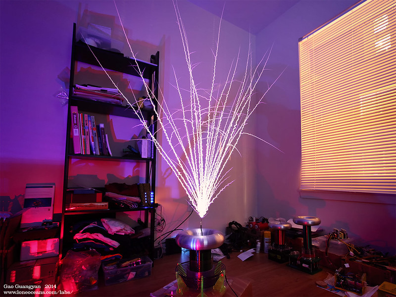
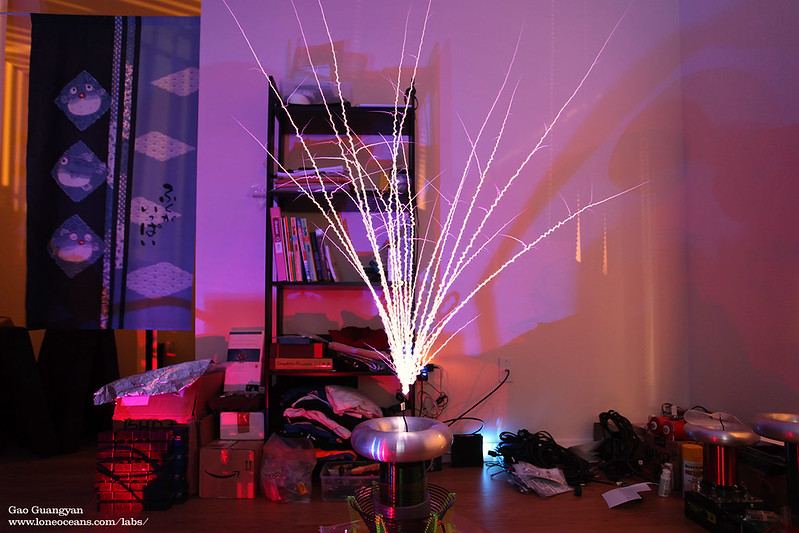
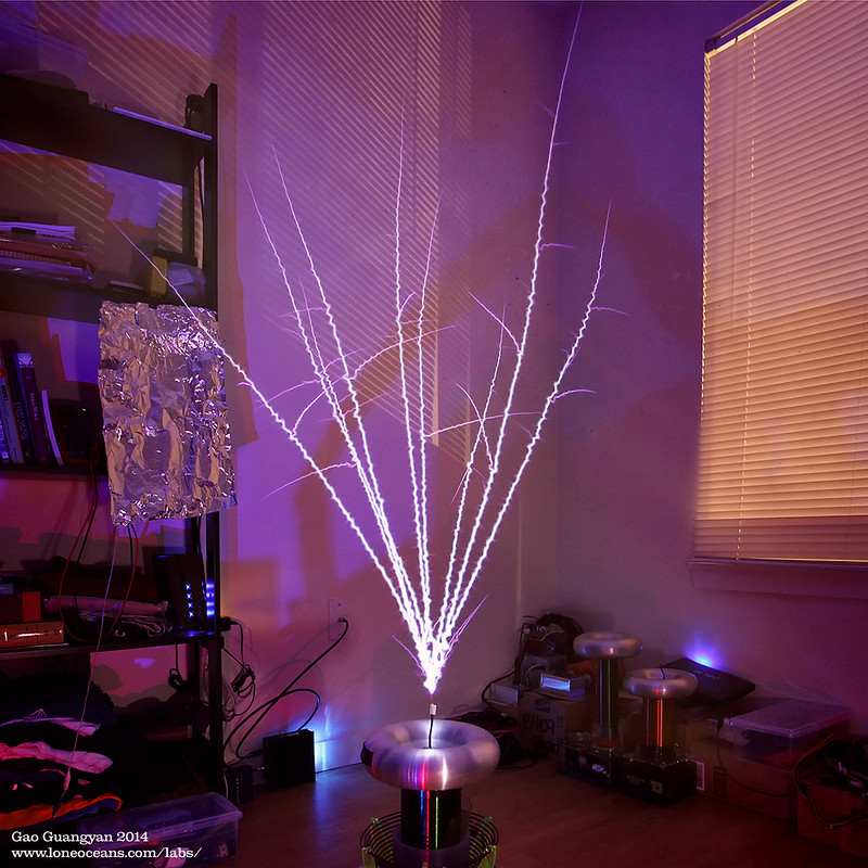
It's alive! It all came together in the end, and without
any tuning at all! Here are
the run parameters for the first light test:
- Bus charged to 180VDC at 6800uF
- Pulse length around 6.2 to 6.5ms to peak of ramp, total ramp time just
over 7ms
- 465kHz to 434kHz running frequency from start to maximum ramp
- Primary current ~100 to 108A at peak
- Spark length around 40 inches (1m)
- OCD conservatively set at around 120 - 125A
- Primary set at turn 7.5 (392kHz) but coil oscillates itself to the
upper pole
It was beautiful and mesmerizing to watch (and hear).
Ramping down really makes the spark much quieter (during OCD trips, it
ends with a harsher bang sound). I found that for reliable operation, I
needed to add a lot of capacitance to my UD2.7 drive up to 1000uF or
more (I used 2000uF in the end just so it would look symmetric!), and
used a beefier 2A 24V SMPS for drive power. This was also because I got
ahead of myself and implemented an under-voltage lock-out on my UD2.7,
and I found that it worked well :-).

Above shows a capture of the primary current (yellow,
0.05V/A) and the buck output into the inverter. The output is quite good
and everything is working as expected. Here you can see the interrupter
pulse about 7.8ms long (probably a bit too long at the end after it
ramps down, so I'll fix my interrupter code soon). In this particular
pulse, the current goes up to about 126A just below my current OCD
limit. The bus floats at about 30V. Note how at the end of the ramp
(where the primary current is about 30A), when the interrupter cuts, the
current in the inductor causes the jump in the bus voltage (remember
this is an async buck), which then decays through my 4.7k bleeder
resistor across my output cap. This has a 3RC value of 406ms, which is
sufficient for the low BPS I am currently running at.
Another note - I was never really sure what sort of load
a high-Z tesla coil would be. The trace above of the primary current
may provide some insight. I realized that the envelop looked very much
quadratic, and sure enough, I fitted a quadratic line to it and it looks
almost perfect (pink line). Now with normal resonance at a fixed bus
input, I noticed that the current rises basically linearly. Since the
voltage in the primary tank goes up linearly, this implies the load
should be constant. With the voltage now increasing from our buck
converter, we can think of the voltage increase as a sum of an
arithmetic series, which is quadratic (n^2+n /2). Perhaps open-loop
control might just work for an even simpler design. I'll be thinking
about this a bit more.
Right now everything is working and I am very glad to
see that all my effort paid off in the end and I reached my goal of 1m
without any tuning, and at only 150V bus voltage! After thinking about
this a bit more, I see no reason why I can't push the coil up to higher
currents, maybe 160A or so. These are the following improvements I plan to
make since my original project goal has now been achieved!
- The buck-layout is quite poor, probably will
re-design it, or even make a small PCB
- Improve drive power for my buck driver with more capacitance and maybe
15V drive
- New goal of 10x secondary length (55" = 140cm)
- A new secondary with lower frequency
- Improve the bleeder circuit for cleaning up the spike (or simply
dropping the ramp to 0 before going up to 30V again)
- Put everything into a nice enclosure
- Maximum current at 160A with maximum of 300V ramp
Looking forward to see how far I can push this project.
:-)
Credits
I would like to thank the following people, for this
project would not have even started without their inspiration and help.
- Steve Ward for his advice on my QCW design (and for
coming up with the first QCW DRSSTC)
- Chris King for advice on buck converter design
- Barmaley from flyback.org for the inspiration to
create a simple yet reliable and small QCW
- Inspiration from zrg's 'Junky QCW' and his QCW with
very impressive output
- The many great tesla coil and high voltage forums on
the internet which gave me valuable advice
- And everyone else who has helped me in one way or another.
More to come soon!
Back to main page
(c) Gao Guangyan 2026
Contact: loneoceans [at] gmail [dot] com |


